Optimizing Stencil Design for PCB Assembly
Stencil Design for PCB Assembly
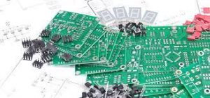
The assembly of a printed circuit board is more complex than simply placing components. It involves the use of a stencil to apply solder paste to parts of the board where an electrical connection is desired. Using a similar process as screen-printing a shirt, a stencil is placed over the board and used to direct the flow of solder paste. The stencil is made from a thin stainless steel sheet that creates openings for each surface mount component in the PCB design. The size and positioning of these openings is vital to a successful PCB manufacturing process and requires careful inspection.
The amount of solder paste that is transported from the stencil apertures to the pads on the PCB is critical for good printing results and proper board assembly. This is called transfer efficiency and it affects everything from fine pitch devices to larger, BGA and flip-chip components. If the amount of transferred paste is too much or too little it can cause smearing, shifting, bridging, open solder joints and other problems.
Stencil materials also impact how well the solder paste transfers from the stencil to the pcb printed circuit board assembly. While stainless steel is the most commonly used material, nickel is a better option for some applications such as high-performance or fine pitch devices. For these applications, a special coating can also be applied like NanoProTek to improve the stencil material’s performance.
Optimizing Stencil Design for PCB Assembly
Aside from ensuring that the correct amount of solder paste is transferred to the PCB pads, the alignment of the stencil with the PCB must be precise as well. To achieve this, registration marks or fiducials are added to both the stencil and PCB. These markings are referenced by the stencil printer to position the stencil accurately over the PCB during printing. This is important because any misalignment can lead to erroneous placement of components on the circuit board.
Another common issue is part-to-part spacing during assembly. This can be caused by not leaving enough space between component boundaries or by not matching the designator labels in the assembly drawing and the actual component. This can result in incorrect placement of polarized components such as diodes or capacitors.
Lastly, some pads on the PCB are designed to dissipate heat through the metal and require a large amount of solder paste to form a proper thermal connection. If too much solder is deposited it can lift the outer leads of the device and cause a short. To prevent this, a special stencil aperture design called a home plate can be used to reduce the solder volume on these large pads.
Vayo’s stencil design check software provides rapid intelligent learning to build a digital SMT stencil library and establish internal company standards for PCB stencil designs. It also offers a fast and comprehensive inspection of stencil designs, which helps to quickly identify discrepancies or violations of internal specifications. By utilizing this tool, engineers can improve their production efficiency and increase quality of the finished product.